
Introduction
In the world of electronics, power supply units play a crucial role in delivering reliable and stable power to various devices. One type of power supply commonly used is the Switched-Mode Power Supply (SMPS). SMPS is widely employed in applications ranging from computers and telecommunication equipment to industrial machinery. In this article, we will delve into the SMPS block diagram, exploring its key components and their functionality.
Table of Contents
- Introduction
- What is an SMPS?
- SMPS Block Diagram
- Input Stage
- Rectifier
- EMI Filter
- Power Factor Correction (PFC) Circuit
- DC-to-DC Conversion Stage
- Switching Transistors
- Transformer
- Output Rectifier
- Output Filter
- Control and Feedback Circuitry
- PWM Controller
- Optocoupler
- Feedback Loop
- Protection Circuitry
- Overvoltage Protection
- Overcurrent Protection
- Short Circuit Protection
- Conclusion
- FAQs
- What is the purpose of an SMPS?
- How does an SMPS differ from a linear power supply?
- Can I replace an SMPS in my computer?
- Are SMPS units energy-efficient?
- What are the advantages of using an SMPS in industrial applications?
What is an SMPS?
Before we delve into the SMPS block diagram, let’s understand what an SMPS is. An SMPS, or Switched-Mode Power Supply, is a type of power supply that efficiently converts electrical power from one form to another. Unlike linear power supplies, which use bulky transformers and dissipate excess energy as heat, SMPS units use high-frequency switching to regulate and convert power efficiently.
SMPS units are known for their compact size, high efficiency, and excellent voltage regulation. These qualities make them ideal for various applications where space is limited and energy efficiency is crucial.
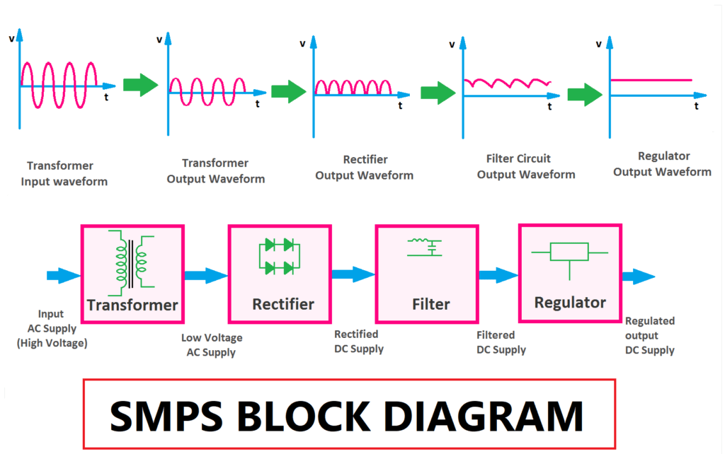
SMPS Block Diagram
The SMPS block diagram illustrates the different stages and components involved in converting the input power into the desired output. Let’s explore each stage in detail.
Input Stage
The input stage of an SMPS block diagram deals with converting the AC input voltage to a usable form for further processing.
1. Rectifier
The rectifier stage consists of diodes that convert the incoming AC voltage into pulsating DC voltage. The rectifier rectifies the alternating current, allowing only one half-cycle of the AC waveform to pass through, resulting in a unidirectional current.
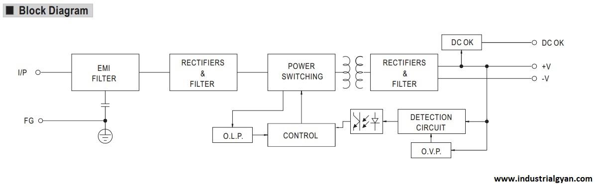
2. EMI Filter
The EMI (Electromagnetic Interference) filter reduces electromagnetic noise generated by the SMPS. It eliminates high-frequency noise from the power lines, on delay timer ensuring compliance with regulatory standards and preventing interference with other electronic devices.
3. Power Factor Correction (PFC) Circuit
The Power Factor Correction circuit improves the power factor of the SMPS by correcting the phase difference between the input current and voltage waveforms. This optimization minimizes reactive power consumption and ensures efficient utilization of the input power.
DC-to-DC Conversion Stage
The DC-to-DC conversion stage is responsible for regulating and transforming the rectified DC voltage to the desired output voltage.
1. Switching Transistors
Switching transistors, often MOSFETs or IGBTs, control the flow of current through the primary winding of the transformer. They switch rapidly on and off, converting the DC voltage into high-frequency AC voltage.
2. Transformer
The transformer is a key component in the SMPS block diagram. It consists of a primary and secondary winding, which facilitates voltage transformation and isolation between the input and output stages. The high-frequency AC voltage from the switching transistors induces a corresponding voltage in the secondary winding.
3. Output Rectifier
The output rectifier stage rectifies the high-frequency AC voltage from the transformer’s secondary winding into a stable DC voltage, ready for utilization by the load.
4. Output Filter
The output filter removes any residual ripple or high-frequency noise present in the rectified DC voltage, ensuring a clean and stable output voltage.
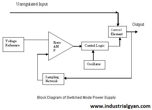
Control and Feedback Circuitry
The control and feedback circuitry monitors the output voltage and adjusts the switching transistors’ operation to maintain the desired output voltage level.
1. PWM Controller
The Pulse Width Modulation (PWM) controller generates the necessary control signals to regulate the duty cycle of the switching transistors. By adjusting the duty cycle, the PWM controller controls the average output voltage.
2. Optocoupler
The optocoupler provides electrical isolation between the high-voltage primary side and the low-voltage secondary side of the SMPS. It ensures the safe transmission of control signals and feedback information.
3. Feedback Loop
The feedback loop compares the actual output voltage with the desired voltage and sends the error signal to the PWM controller. The PWM controller then adjusts the switching transistors’ duty cycle accordingly to regulate the output voltage.
Protection Circuitry
The protection circuitry safeguards the SMPS and the connected devices from potential faults or abnormal operating conditions.
1. Overvoltage Protection
The overvoltage protection circuit monitors the output voltage and disconnects the power supply if the voltage exceeds a predetermined threshold, preventing damage to the load.
2. Overcurrent Protection
The overcurrent protection circuit senses the current flowing through the SMPS and interrupts the power supply if the current exceeds a safe limit, protecting the components from excessive stress.
3. Short Circuit Protection
The short circuit protection mechanism detects a short circuit in the load and shuts down the SMPS to prevent further damage.
Conclusion
In conclusion, understanding the SMPS block diagram helps us grasp the functionality of each stage and component involved in converting electrical power efficiently. The input stage prepares the power for processing, the DC-to-DC conversion stage transforms and regulates the voltage, the control and feedback circuitry ensures stable operation, Power factor improvement and the protection circuitry safeguards against faults. With their compact size, high efficiency, and reliable performance, SMPS units have become the preferred choice for a wide range of electronic devices and industrial applications.
FAQs
- What is the purpose of an SMPS? An SMPS is designed to efficiently convert and regulate electrical power for various electronic devices, providing a stable and reliable power supply.
- How does an SMPS differ from a linear power supply? Unlike linear power supplies, SMPS units utilize high-frequency switching and offer higher efficiency, smaller size, and better voltage regulation.
- Can I replace an SMPS on my computer? Yes, you can replace an SMPS in your computer if it is compatible with the required power specifications of your computer components.
- Are SMPS units energy-efficient? Yes, SMPS units are highly energy-efficient due to their switching nature, resulting in reduced power dissipation and improved overall efficiency
- What are the advantages of using an SMPS in industrial applications? Some advantages of using SMPS in industrial applications include compact size, improved energy efficiency, higher power density, and better reliability compared to traditional linear power supplies.
You can Follow us on LinkedIn

I am a highly motivated and skilled individual with a passion for Electrical engineering. I have 1 year of experience in Robotics and Electrical engineering, which has allowed me to develop a strong set of skills in PLC, Painting Robots, SCADA. I am a quick learner and am always looking for new challenges and opportunities to expand my knowledge and skills. I am a team player and enjoy working with others to achieve a common goal. Successfully completed many projects for a various clients in the automobile sector.
Thank You